DIY PCB manufacturing
I used to use the toner transfer method for PCB manufaturing for a few years but I could never achieve consistent quality. I've read some very positive reviews of using UV exposure boxes and some tutorials of modding old scanners into one. Luckily I managed to buy a second hand Philips facial tanner at a very low price. Buying the UV tubes alone would have cost me more normally.
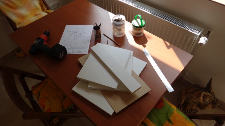
I designed a really simple box with a glass top and started building. Here are all the necessary parts:
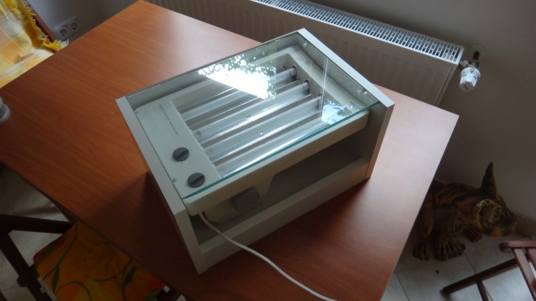
And here's the finished box with the tanner inside:
I tested the exposure box with a simple test pattern and used a piece of paper to cover some part of the PCB. The paper was moved to the left every minute by one "block" in order to find the perfect exposure time.
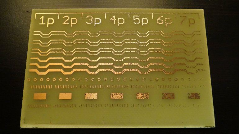
After etching and developing, it was clear that this was way too much time so I did a second test. This time I moved the paper every 10 seconds.
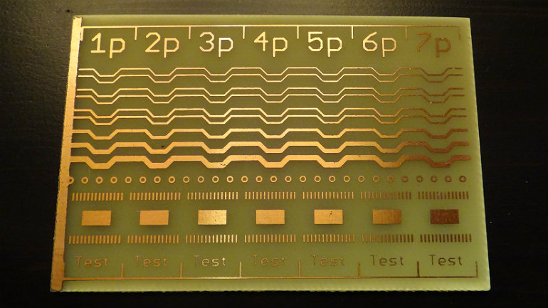
The ideal exposure time seemed to be 40-60 seconds with this configuration. Here's an evaluation board for MAX8815A step-up converter made with this box:
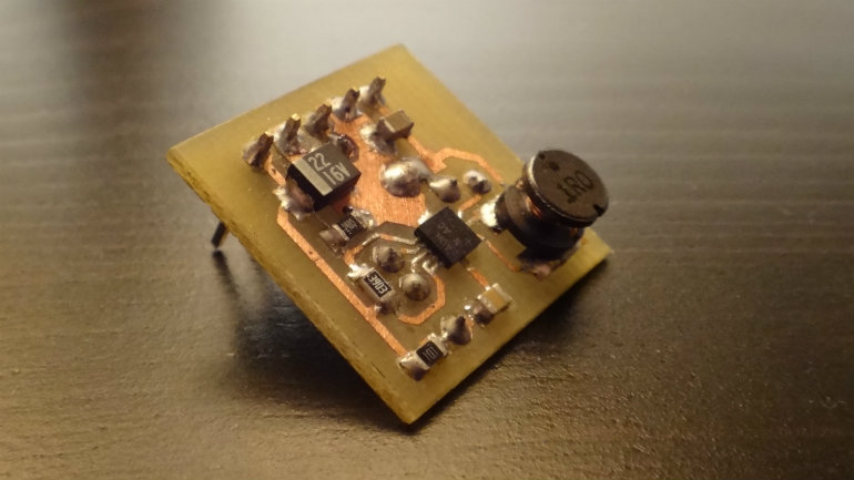
The tiny IC in the middle is a 3x3 mm TDFN package with 10 pins!
Description
Easy DIY PCB manufacturing with a UV exposure box.